CPU / CPU Subsystem
 Home / CPU / CPU Subsystem
CPU / CPU Subsystem
The processor subsystem of an SoC is a complex and essential component in modern electronic devices. As technology advances and the demand for high-performance and power-efficient devices increases, the design of the processor subsystem in an SoC continues to play a critical role in determining the success of the device.
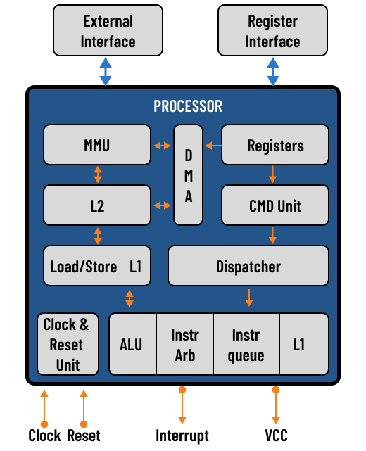
The processor subsystem of an SoC includes the processor, cache memory, system memory, and various other components required to support the operation of the Processor. The processor in an SoC is typically a low-power, high-performance processor that is optimized for the specific application of the device.
The processor subsystem consists of several key components, including the processor chip, cache memory, and system memory. The processor chip responsible for executing instructions and performing calculations. The processor contains multiple cores, each capable of executing instructions in parallel, which allows for faster processing speeds.
Cache memory is a type of high-speed memory that stores frequently accessed data and instructions. It acts as a buffer between the processor and the slower system memory, helping to improve performance by reducing the amount of time the processor spends waiting for data to be retrieved from system memory.
Other components in the processor subsystem of an SoC include power management units, clock generators, input/output controllers, and various other components required to support the operation of the processor. These components are designed to work seamlessly with the processor to optimize performance and power consumption for the specific application of the device.
Processor Unit Features
The 4 main architectural characteristics of the processor are:
- Task/ Thread level parallelism
- Depth-first hardware scheduling-Dynamic execution
- Minimal use of off-chip memory
- Fully programmable Architecture.
- Two 512b native read interfaces and one 512b native write interface to access memory.
- APB slave interface for register access
| Attribute | Value |
|---|---|
| Interface Type | AXI |
| Read Address | 64 Bit |
| Write Address | 64 Bit |
| Read Tag | 8 Bit |
| Write Tag | 8 Bit |
| Outstanding Read transactions Per port | 256 |
| Outstanding Write transactions | 32 |
| Read Data width | 512 Bit |
| Write Data width | 512 Bit |
Processor Capabilities
Executed multiple CPU based SoC designs in Delivery Ownership environment including design, integration, verification, DFT, and physical implementation.
Successfully set-up and efficiently operating an ODC for a processor IP multinational corporation.
Engineers with exposure to CPU internals and subsystem verification, deployed on related customer projects
Ongoing expansion of design and verification engineers with exposure to areas including but not limited to.
- Knowledge of a CPU architecture such as x86, RISCV, ARM, and custom processor
- SoC fabric, memory controller, security, caches, coherence
- Instruction set verification and Random Instruction Sequencing (RIS) and testing
- Cache coherence, memory ordering and consistency, prefetching, Dynamic execution, speculative execution, Thread level parallelism, and memory translation
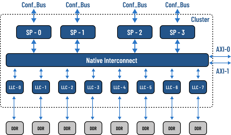
CPU Cluster
Cluster is top level integrated module consisting four instances of Streaming processor, 8 Last level caches and a native interconnect.
The SPs, native interconnect and LLC Caches can work in different clock domains, so there are synchronizers placed between the modules in different domains.
Design and development of the Native interconnect and integration of the all the components is the scope.
Native interconnect implements the DDR memory map and routes the memory access transactions to appropriate LLC’s.
It also has 2 AXI slave ports connecting to the SoC interconnect.