High Speed I/O Interface
 Home / High Speed I/O Interface
High Speed I/O Interface
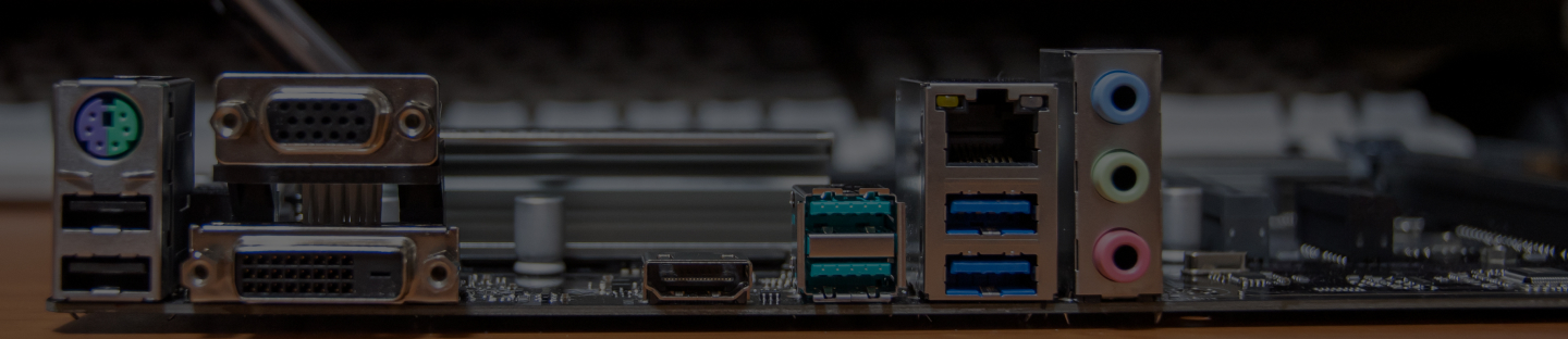
The high-speed input/output (IO) subsystem in System-on-Chips (SoCs) is critical to the performance of the entire system. High-speed IO interfaces include protocols such as PCI Express, USB, SATA, and Ethernet, which are used to connect to high-speed devices such as solid-state drives, network cards, and external graphics cards.
To ensure optimal performance of the high-speed IO subsystem, several design techniques can be implemented. One approach is to use dedicated hardware blocks, such as DMA engines and hardware accelerators, to offload the processing of data transfers from the CPU. This reduces the overall latency and improves system performance.
Another approach is to use advanced caching and buffering techniques to optimize data flow and reduce the impact of high-speed IO traffic on the rest of the system. This can include techniques such as read-ahead and write-behind caching, which can help reduce the number of transactions required for data transfers and improve the overall efficiency of the system.
Additionally, software optimizations can also be employed to improve the performance of the high-speed IO subsystem. This can include techniques such as interrupt coalescing, which groups multiple interrupts into a single interrupt, reducing the CPU overhead required to handle them.
Finally, signal integrity and power integrity must be carefully managed to ensure reliable high-speed data transfers. This can involve techniques such as signal equalization, termination, and voltage regulation, which help minimize noise and distortion in the high-speed signals.
In summary, a well-designed high-speed IO subsystem is critical for delivering optimal performance in modern SoCs. By using a combination of hardware and software optimizations, designers can ensure that the IO subsystem operates efficiently and reliably, maximizing the overall system performance.
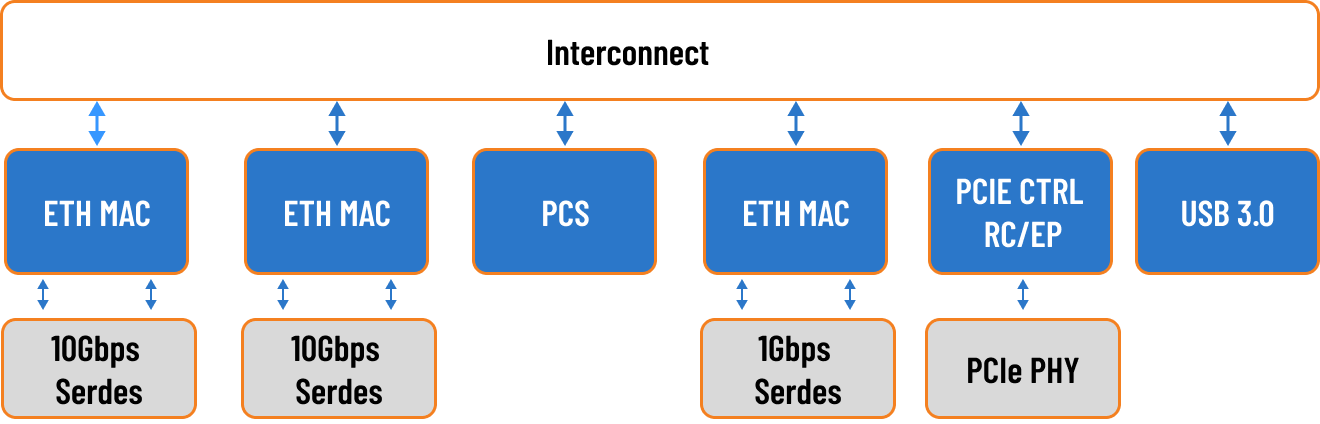
High speed IO subsystem design containing IP’s like PCS, PCIe,MAC etc.
The interconnect and LS IP’s will work in different clock domains, so there are synchronizers placed between the modules in different domains.
Owning the HSIO subsystem which includes, designing, verification and implementation.
It also has AMBA slave ports connecting to the SoC interconnect.
Lot of manual and custom placement is required for data link and transaction layer logic
CTS to be build with spine structure to meet the skew requirements
Support Activities
Verify subsystem connectivity and basic function
Synthesize all RTL
Create subsystem testbench with standard VIPs or new ones as needed
DFT insertion (scan/lbist, MBIST & ijtag)
Check performance of major interfaces
Place and Route RTL blocks and 3rd party hard macros
Floorplan each subsystem per top level plan
Iterate as necessary for timing closure
Create clock and placement constraints as necessary
Perform RTL/gate equivalence checks
Perform all LVS and DRC
Perform ECOs for SOC timing and floorplan closure and IP