Memory Subsystem
 Home / Memory Subsystem
Memory Subsystem
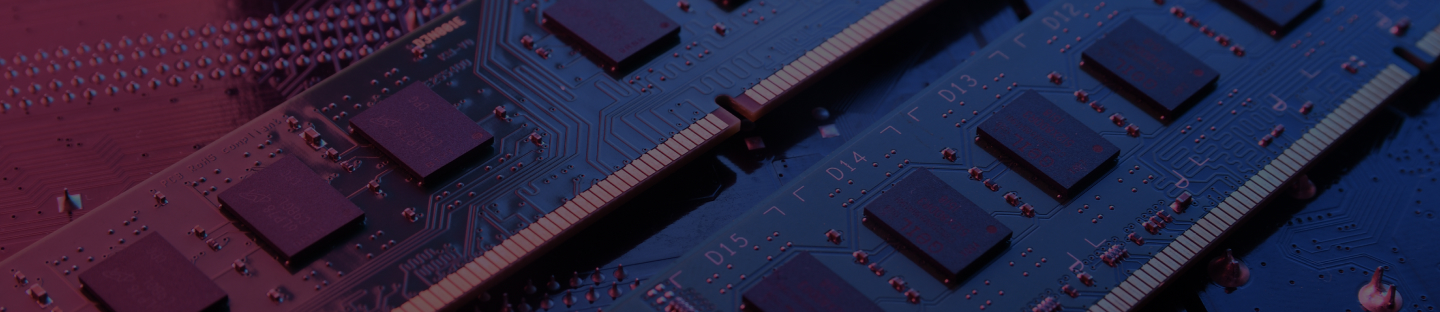
A memory subsystem in a System-on-Chip (SoC) is a crucial component that manages the flow of data between the processor and various types of memory devices such as RAM, ROM, and cache. The memory subsystem is responsible for ensuring that data is accessed and transferred quickly, reliably, and efficiently.
The memory subsystem typically consists of several components, including memory controllers, buses, and interfaces. Memory controllers are responsible for managing the flow of data between the processor and various types of memory devices. They also control the timing and sequencing of memory accesses to ensure that data is transferred without errors.
Interfaces are used to connect the memory subsystem to external devices such as hard drives, network interfaces, and other peripherals. They provide a standard interface that allows these devices to communicate with the memory subsystem, enabling them to access data stored in memory.
The memory subsystem also includes various types of memory, including Random Access Memory (RAM) and Read-Only Memory (ROM). RAM is used for temporary storage of data and program code, while ROM is used to store firmware and other types of read-only data.
In summary, the memory subsystem in a SoC is a complex component that manages the flow of data between the processor and various types of memory devices. It includes memory controllers, buses, interfaces, and various types of memory, including cache, RAM, and ROM. Its efficient operation is critical for ensuring that the SoC operates reliably and efficiently.

- Memory subsystem design contains embedded DDR Queue, Memory controller and PHY. eDQ is designed to provide fast and efficient access to memory, while minimizing latency and maximizing throughput.
- eDDR queues often use specialized hardware and software to optimize memory access, such as using pipelining or caching techniques.
- The interconnect and Memory subsystem work in different clock domains, so there are synchronizers placed between the modules in different domains.
- Owning the Memory subsystem which includes, designing, verification and implementation.
- It also has AMBA slave ports connecting to the SoC interconnect.
- CTS to be build with spine structure to meet the skew requirements
Support Activities
Verify subsystem connectivity and basic function
Synthesize all RTL
Create subsystem testbench with standard VIPs or new ones as needed
DFT insertion (scan/lbist, MBIST & ijtag)
Check performance of major interfaces
Place and Route RTL blocks and 3rd party hard macros
Floorplan each subsystem per top level plan
Iterate as necessary for timing closure
Create clock and placement constraints as necessary
Perform RTL/gate equivalence checks
Perform all LVS and DRC
Perform ECOs for SOC timing and floorplan closure and IP